There is great demand for more sophisticated technologies in metrology for the next generation of semiconductor devices. This is fueled by the desire for powerful integrated circuits that are needed for the latest applications in artificial intelligence and the Internet of Things (IoT). The semiconductor industry continues to deliver such devices, but it is becoming challenging to increase manufacturing yields while producing advanced technology nodes with nanometer-scale features.
New metrology tools are needed to make accurate measurements of these device structures while keeping the manufacturing yield high, costs low, and product development fast. Let’s find out what semiconductor metrology is, why it’s important, how it’s performed currently, and why there is a need for new metrology solutions for the next generation of semiconductor devices.
The Metrology of Semiconductor Devices
Semiconductor device manufacturing is a complex process that takes place over a period of two months with hundreds of procedures carried out during that time. At critical steps during this process, special tools are used to evaluate the nanometer-scale structures and verify they have been produced according to the target physical dimensions.
The Importance of Metrology
If the measurements of these microscopic structures are not within a specified range, the final product may not perform as intended. The measurement processes used to quantify physical sizes, characteristics, and distances between features are called dimensional metrology or simply metrology, and it is absolutely crucial to ensure the desired yield is maintained.
Examples of Metrology
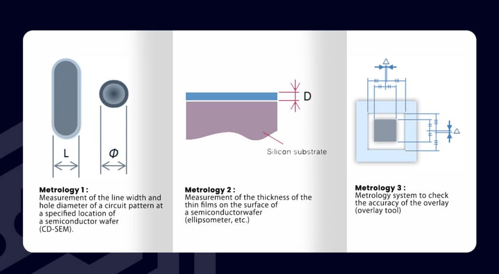
One example of metrology performed on specific points of a semiconductor wafer is the line width and hole diameter of a circuit pattern. Another type of measurement is the thickness of the thin films that are made on the surface of a silicon substrate. There are further measurements done to verify the accuracy of the shot overlay for first and second-layer patterns that have been transferred onto the surface of a semiconductor wafer. For more advanced logic devices, gate height, sidewall angle, and fin height also need to be measured.
Metrology vs Inspection
Metrology is not to be confused with wafer inspection which is performed during manufacturing to detect the presence of contaminants, and manufacturing defects that can also compromise the performance of a device. There is also automated test equipment used to check whether the electrical characteristics of manufactured chips meet specifications. These tools work together with metrology equipment for quality control in semiconductor manufacturing.
Best Measurement Methods Used by the Semiconductor Industry
Various technologies and tools are used by semiconductor manufacturers to conduct the necessary meteorological procedures. Here are a few examples of the best electron beam-based and optical wafer metrology sensors used today, as well as a few cutting-edge methods that are still in the research and development phase.
Critical Dimension Scanning Electron Microscope (CD-SEM)
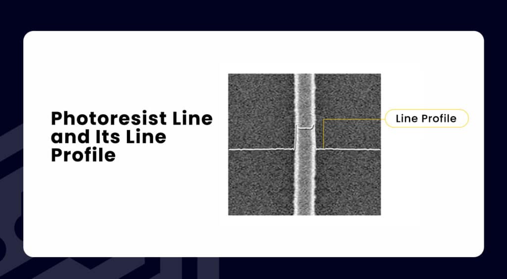
This technology is currently the most widely used metrology tool in the industry. The Scanning Electron Microscope can be used for top-down measurements of planar transistors. The device works by using a focused beam of electrons to perform the scanning on the wafer surface. The resulting line profile helps in obtaining accurate measurements of surface structures.
Early models had difficulty measuring FinFETs because they could image the fin height and sidewall angle of these components. More recently, beam-tilt capabilities have been added to newer models by CD-SEM manufacturers to get these additional measurements. Others have integrated back-scattered electron detectors which are capable of presenting a clear picture of the surface topography and even determining the composition of next-generation devices.
Atomic Force Microscopy (AFM)
In this method, a cantilever with a tiny needle scans the surface of a wafer and creates a three-dimensional measurement of surface structures. The resolution of AFM can go up to 0.1 nanometres. Atomic Force Microscopy is typically slow and not used as much as CD-SEM in fabrication plants, although faster models are currently being developed. It is also used outside the world of semiconductors in many different fields to scan materials. For more on different types of microscopes used for inspection, read What Does A Semiconductor Microscope Do?
Optical Scatterometry
This method is also one of the most popular inline metrology tools because it is not only precise but quick and non-destructive. It works by illuminating the semiconductor device with a light and then measuring the intensity of light scattered by the surface. It is used mainly for measuring dimensions like side-wall angles, line width, and height of structures.
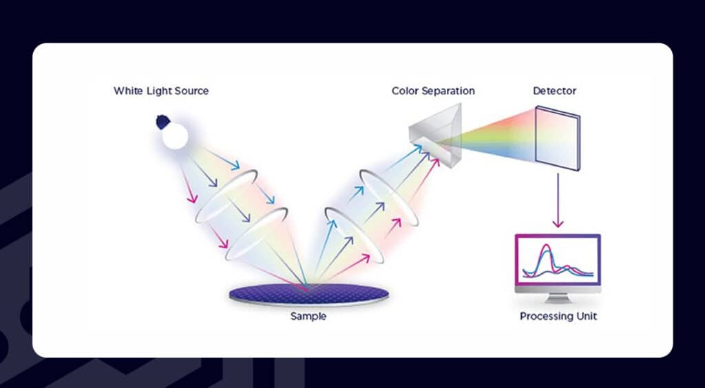
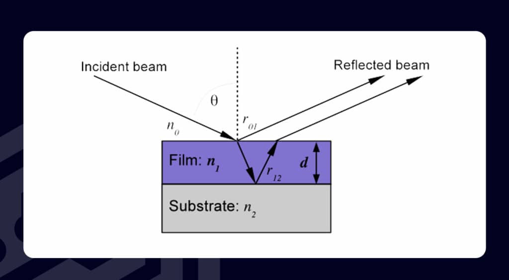
Spectroscopic Ellipsometry
Ellipsometry is another non-destructive optical method that is used to take measurements of thin films that are present on the surface of wafer substrates. Properties such as layer thickness, surface roughness, surface composition, optical anisotropy, and optical constants can be determined through this method. It is used primarily for the metrology of memory and logic-based microchips.
Model-Based Infrared Reflectometry (MBIR)
In this method, infrared wavelengths are used instead of visible light. The amount of infrared light reflected off the sample device is measured and compared with that of a model. Film stacks found in DRAM and 3D NAND devices are measured this way.
Small Angle X-ray Scattering (SAXS)
This is one of the latest techniques in metrology that is still in research and development. It shows great potential for measuring the edge roughness, pitch walking, and average shape of periodic nanostructures in new devices. What is currently limiting this technology is that the brightness of the X-ray sources used is not bright enough for good measurements.
Reaching the Fundamental and Engineering Limits of Semiconductor Devices
As semiconductor devices get smaller, they are now approaching the fundamental limits determined by their physical and chemical properties. These smaller devices are already operating right at the edge of their heat dissipation, carrier mobility, and fault tolerance thresholds. This means that the nanometre scale structures will need to be scrutinized and measured even more diligently and accurately.
Metrology for the Next Generation of Semiconductor Devices
The sophisticated measurement methods needed for these next-generation devices are pushing metrology tool-makers to develop ever more advanced technologies and improve their existing equipment to provide even more capabilities. Apart from the metrology tools, smart manufacturing methods are now starting to be utilized by the semiconductor industry with advanced algorithms that interpret measurements and provide more insight to manufacturers. To learn more about semiconductor manufacturing, the equipment used, and the latest industry news, check out Inquivix Technologies!
FAQs
Metrology is about verifying the physical dimensions of surface structures in semiconductor devices, while the inspection is performed to detect contaminants and manufacturing defects.
Line widths, hole diameters, and thickness of thin films are examples of measurements taken in semiconductor metrology. For more advanced devices, the gate height, fin height, and sidewall angle may also need to be measured.
The latest semiconductor devices are approaching their engineering limits like carrier mobility, heat dissipation, and fault tolerance thresholds. They require more accurate methods to ensure their structures are manufactured according to specifications.