
As the global hunger for consumer electronic devices like smartphones, 4K televisions, and wearable tech increases along with emerging fields that are powered by machine learning and blockchain technology, there has never been more demand for semiconductor-based devices.
With this demand comes ever-mounting pressure on device manufacturers to ensure a steady supply. On top of this, integrated circuits (ICs) keep shrinking in size and growing in complexity as manufacturers keep attempting to cram more computing power into smaller and smaller chips.
This makes high-volume manufacturing challenging since steps need to be taken during the production process that guarantees good quality control. Semiconductor device structures need to be accurately replicated since the presence of the tiniest defects on wafer surfaces could compromise the end product. Therefore a robust imaging system is needed for defect inspection.
While many semiconductor imaging techniques have appeared over the years, not all of them are suitable for wafer inspection during manufacturing. Let’s find out the limitations of some of these conventional imaging techniques, and why they don’t work well during the manufacturing process. We’ll also discuss the industry-standard imaging methods used for defect inspection of wafers, as well as how they can be improved to get around the challenges of inspecting smaller and more sophisticated ICs of tomorrow.
Why The Wafer Inspection Process Is Important
Wafer inspection is an important part of the manufacturing process for semiconductors. As devices get smaller and smaller, their tolerance for manufacturing defects becomes lower, with even the tiniest imperfections on a wafer causing it or its end product to be unusable. Therefore defects are costly for a manufacturer, and it is in their best interest to use the latest technology available to detect these defects as quickly as possible without slowing down the production process too much.
Not only do well-known defects like crystal defects and contamination from dust particles continue to have an impact, but manufacturers are also discovering entirely new defect types as they work near the nanometer scale. As newer, smaller, and more advanced integrated circuits are developed, better defect detection methods are required to inspect them.
While semiconductor cleanrooms can mitigate issues like contaminants to some degree by carefully controlling the manufacturing environment, and semiconductor reliability testing can improve the production process to reduce the number of pattern defects occurring, they cannot completely eliminate them. Therefore defect detection becomes a vital aspect during manufacturing, requiring tools designed specifically for wafer inspection.
Why Wafer Inspection Methods Used In Failure Analysis And R&D Won’t Work During Manufacturing
Defect inspection can be done with electron beam microscopy techniques like the Scanning Electron Microscope (SEM) and the Transmission Electron Microscope (TEM). These electron beam technologies offer high spatial resolution and material contrast compared with optical systems. However, their scanning speed is low, making them unfit for use in a production environment to keep up with the sheer volume that needs to undergo inspection.
That being said, an electron beam-based inspection tool is a great way to supplement semiconductor failure analysis efforts to understand how integrated circuit devices fail. An electron beam inspection tool can also be used for qualification purposes during process development when new tools or raw materials are introduced. Electron beam tools can find defects at 10 nanometers and lower, and new models are being developed to improve their throughput.
To learn more about the different types of microscopes used from optical to the electron beam and atomic force microscopes, read What Does A Semiconductor Microscope Do?
Imaging Techniques Used For Defect Inspection In Wafers
Wafers are subject to defect inspection at various stages of production. It’s done first at the wafer manufacturing plant to qualify non-patterned or bare wafers, then again at the next factory where chip makers take over and turn them into integrated circuits. Different types of optical systems are used for defect detection at each step of the process by analyzing the light reflected or light scattered during the process. They are typically chosen for their relatively high throughput, speed, and lower cost compared to other methods like electron beam microscopy.
Non-Patterned Wafer Inspection
A non-patterned or bare wafer has a uniform surface and has not yet been processed to create the circuitry that would turn it into an integrated circuit (IC). A defect inspection is carried out first by the semiconductor wafer manufacturer to ensure only qualified products are sent out. The IC manufacturer will perform their own defect inspection before turning the bare wafer into functioning microchips to separate any pre-existing defect types from those arising from their own production processes.
How Non-patterned Wafer Inspection Is Done
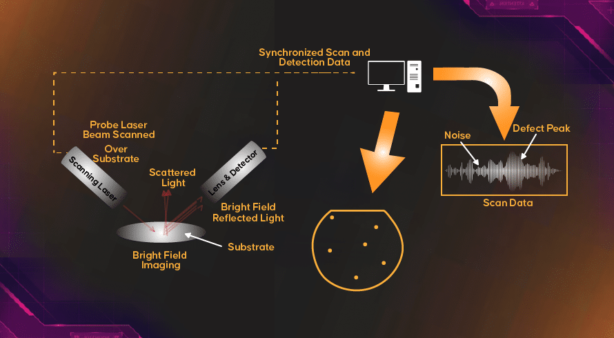
The non-patterned wafer is rotated and a laser beam is directed at its surface to scan it radially. The wafer reflects this light as a mirror would, at a specific angle, and this type of reflection is called ‘specular reflection’. Contaminants like particles or any other type of defect present on the surface have different optical properties, causing part of the light reflected to be scattered away from its usual path. Through dark field illumination, scattered light can be detected. Alternatively, bright field illumination can reveal the loss in intensity of the reflected light.

The intensity of the scattered or reflected light of the laser beam can be measured by using a Photo Multiplier Tube (PMT) or Charge Coupled Device (CCD) type detection system. Using the radial position of the laser beam and the rotational position of the non-patterned wafer, the exact position of the defect detected can be determined. These coordinates and measurements will generate a map that allows manufacturers to not only find defects but to keep track of their size and location on the rotating wafer surface.
The various components used such as the wafer stage which handles the movements of the delicate rotating wafer during scanning and the optical equipment that performs the scan need to be extremely precise and capable of repeatable movements. This is done through sophisticated motion control systems attached to these components.
Generally, defect detection in bare wafers is done using dark field illumination, since the image rendering (rastering) is done faster than bright field. This allows for quicker production and ultimately a higher throughput. Apart from the general wafer inspection that is done at very high volumes, other applications require slightly more advanced equipment.
Going Sub 100 Nanometer With Deep Ultraviolet
Quality assurance needs to be done on wafers coming in from a supplier and the process tools used later for high-volume production need to be monitored and qualified as well. These evaluations are carried out by sophisticated sub-100 nanometer inspection tools that operate on the same principles to find defects as those used in high-volume production. What separates them is the use of Deep Ultraviolet (DUV) illumination techniques to enhance their optical systems.
An inspection tool that can detect defects at the sub-100 nanometer level has all kinds of new challenges to contend with. The signal-to-noise ratio (SNR) of the scattered lightwaves is reduced at these scales due to issues like microroughness of the wafer surface and ambient humidity. These advanced defect detection tools use image analysis algorithms, the polarization of the signal, and optical spatial filtering to overcome these challenges.
Patterned Wafer Inspection
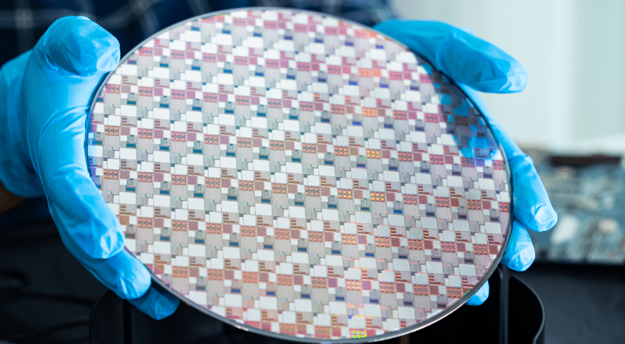
A patterned wafer is one where functional circuit blocks have been fabricated. Each of these blocks is called a ‘die’. A single wafer contains many of these blocks, each a copy of the same circuit arrangement. The blocks are then cut from the patterned wafer and then packaged to form a finished integrated circuit. Both dark field and bright field illumination techniques as well as a combination of both can be used to detect defects in a patterned wafer.
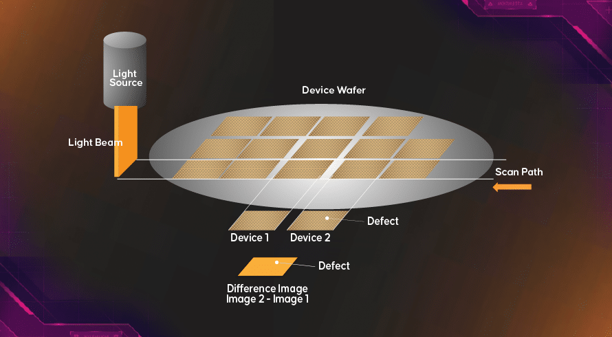
How Patterned Wafer Inspection Is Done
A patterned wafer inspection tool works by comparing a single die on the wafer surface to a ‘golden die’ that is already known to not contain any defects. Software tools are used which can subtract the test die image from the golden die image. The subtracted image will indicate any defects present on the test die, and a defect map can be prepared for the entire wafer. Just like in non-patterned wafer inspection, the patterned ones also require precise motion control mechanisms to carry out these tasks. The defect detection process for a patterned wafer is much slower than that of a non-patterned one.
While traditionally done using visible light, a patterned wafer inspection tool utilizes Ultraviolet frequencies with the latest equipment now using Deep Ultraviolet (DUV) to scan near the 65-nanometer range. DUV wafer inspection tools have proven to be very effective at discovering pattern defects at the sub-100 nanometer scale such as shallow trench photoresist micro bridging, contact etch defects, and isolation voids. Using broadband illumination with visible, UV, and DUV for bright field detection, flash devices, as well as DRAM chips can be inspected at the 55-nanometer range.
Issues With Deep Ultraviolet And Use Of Broadband Plasma Illumination
Since DUV-based methods are well understood and have lower costs and high throughput than others, they have been very popular among manufacturers. However, some in the industry have claimed that DUV illumination when used with dark field methods is not sensitive enough for identifying defects below 65 nanometers. There have also been issues like laser ablation of the surface where surface materials are removed from small or fragile structures when the laser beam performs the scanning. Broadband plasma illumination methods may prove key to solving these issues, and may even allow defect detection at the sub-10 nanometer scale.
Reticle Inspection
While a defect present on a non-patterned or a patterned wafer spells bad news for the end product that contains that defective region, a defect present in a reticle will be passed on to every wafer that is processed by it. This is why.
What Is A Reticle?
Through a process called photolithography, the non-patterned Silicon substrate is exposed to light passing through a photomask. Different sets of photomasks contain the patterns that need to be layered into the wafer one by one. This is how the tiny circuits on the surface of the wafer are created. A reticle is a type of intermediate photomask used to copy photomasks used during production.
This means that if one reticle is compromised, thousands of ICs manufactured from it could contain manufacturing flaws, causing the whole batch to be rendered useless. Therefore reticle inspection is an important part of the manufacturing process that is performed alongside wafer inspection.
How Defect Detection In Reticles Are Done
Defect detection in reticles is further complicated by the reflective properties of its design and needs to be inspected using transmitted light rather than light reflected. The inspection procedures are based on the same principles used for a patterned or non-patterned wafer with any defect causing the light to scatter from its usual path.
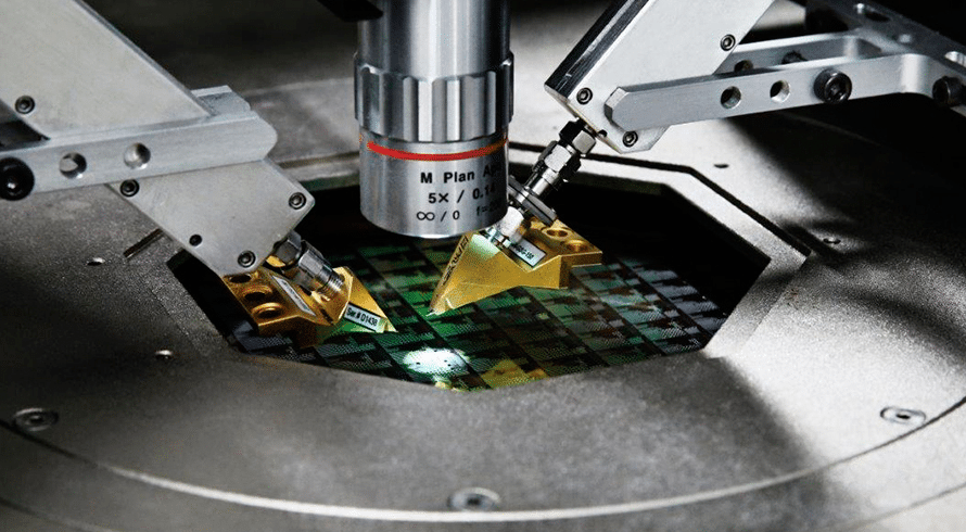
Visible light and Ultraviolet can be transmitted through a sample to identify defects on a blank or patterned reticle with Deep Ultraviolet used at the sub-100 nanometer level. It is standard practice in the semiconductor industry to routinely check reticles throughout the production process. Precise motion control systems are needed to handle the inspection of reticles and image analysis algorithms are employed to obtain better results. Furthermore, electron beam methods can be employed since a high throughput is not an issue with reticles.
How To Get A Better Semiconductor Image For Defect Inspection

While optical methods are used all the time to maintain high throughput, their resolution is limited even with DUV-type illumination. Electron beam and atomic force microscopy offer great resolution but poor scanning speed. A new method called Line-Scan Hyperspectral Imaging (LSHI) was recently developed by Samsung Electronics which aims to improve the resolution of optical inspection.
In LSHI, a rectangular beam of light illuminates the inspection zone of the wafer, and the light reflected is collected into a special module that can separate it into its constituent frequencies. Imagine a high-tech prism that can split the incoming beam of light. These are then analyzed by a set of cameras, each precisely calibrated to detect a specific spectral range. LSHI allows the measurement of massive amounts of both spatial and spectral data. The field of view is said to be improved as well, which has the potential to increase throughput. The downside so far seems to be that this technique requires a more sensitive detector and more stability in the light source.
Building Better Semiconductor Devices Through Defect Inspection
While conventional methods using optical inspection tools are still in use, new techniques like LSHI are being developed all the time. Though they require improved precision motion controls, extra sensitive cameras, and light sources that are more stable, these could be solved as more sophisticated equipment becomes available across the industry.
As more advanced semiconductor imaging techniques are employed for defect inspection, it smooths out issues during production, helping reduce waste and costs for the manufacturers. This translates to delivering new and reliable microchips that power the next generation of electronics that will shape the world of tomorrow.
For more on semiconductors and the latest news from the industry, check out Inquivix Technologies!
FAQs
Wafer inspection is done during the manufacturing of semiconductors to check for the presence of pattern defects and contaminants like dust particles in the wafer.
Metrology concerns engineering analysis methods used to verify that the physical and electrical performance of semiconductors is meeting production requirements, while an inspection is about finding defects such as particles or surface flaws that can compromise the performance of the end product.
Defect inspection is what allows manufacturers to find defects and contaminants like dust particles on the surface of a wafer which can compromise the performance of the integrated circuits fabricated on it.