
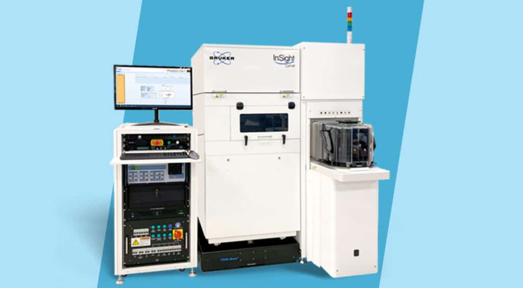
A semiconductor microscope or wafer inspection microscope is a critical quality control aspect of the manufacturing process. The tiniest defects like cracks in the delicate Silicon wafers or impurities present in the raw materials could make the final product unusable in practical applications. This can result in wasted resources and huge costs for the manufacturers. This is why the semiconductor industry utilizes a wide variety of microscopes as part of their inspection procedure during manufacturing.
Let’s find out why a manufacturer needs to use semiconductor microscopes, the various types of microscopes and cameras used for the inspection of semiconductor materials, how they help identify defects in the wafers, and why it’s so important to detect these issues early in the process.
What Is A Semiconductor Or Wafer Inspection Microscope?
Integrated circuits known as ICs are made from semiconductors. They are key components present in nearly every piece of modern technology, from smartphones, and virtual-reality headsets, to medical devices and the latest automobiles. There are many types of materials used by the semiconductor industry with Silicon wafers being one of the most widely used types of material to manufacture these integrated circuits.
Highly pure and monocrystalline Silicon ingots are synthetically made in factories in boule or cylindrical shapes. A circular thin slice of this ingot becomes a wafer. These wafers undergo many different stages in the semiconductor production process such as masking, etching, ionization, and more. These procedures are what create the microscopic circuits on the surface of a Silicon wafer. There could be millions of components on a single wafer. These wafers are later cut to form individual integrated circuits.
Semiconductor microscopes are what manufacturers use during production as tools for the inspection of these wafers. There are many types of microscopes employed which utilize different methods for analysis such as optical microscopy, electron microscopy, infrared microscopy, and atomic force microscopy to name but a few. Each has its own advantages. They all play a key role in the inspection procedure to detect any issues in the semiconductor products.
Why Wafer Inspection Is So Important for Quality Control?
During the many stages of semiconductor production like growing, etching, and cutting into individual ICs, there are stresses that affect the delicate Silicon wafers. These stresses could cause cracks to appear on the surface. There could also be impurities present in the raw materials that affect the finished product as well as various contaminants introduced during manufacturing.
Whether it’s contamination by dust particles or cracks in the wafer, this can seriously compromise the quality of the integrated circuits produced. The microchips may even be unusable, and since semiconductor manufacturing is so expensive, it can be a major issue for the companies that operate these factories. With so much demand for semiconductor components in everything from the LED flat panel displays that make up your television to robots used in industrial automation, a manufacturer cannot afford a whole batch of their products to be defective.
One of the solutions used by the semiconductor industry to reduce the chance of contamination is to have production take place inside specially designed cleanrooms. These cleanrooms keep the manufacturing environment at the optimum temperature and humidity while using filters to reduce dust and other particulates during production. To learn more, read What Is a Semiconductor Clean Room and What Is It For?
While cleanroom environments can reduce contaminants, quality control requires careful inspection of the wafers through each stage of production. Microscopes are the crucial inspection tools used by manufacturers to identify cracks and any other issues present in their semiconductor products. This allows them to find solutions to these issues and improve their yield.
The Types Of Microscopes And Their Applications In The Semiconductor Industry
Research and development in the field of microscopy have resulted in many different methods that help in the failure analysis of semiconductor materials. They all have unique features and advantages, allowing semiconductor makers to observe the smallest details on their wafers. These instruments help them identify any defects present in the wafers and maintain a high standard of quality for their products.
Optical Digital Microscope
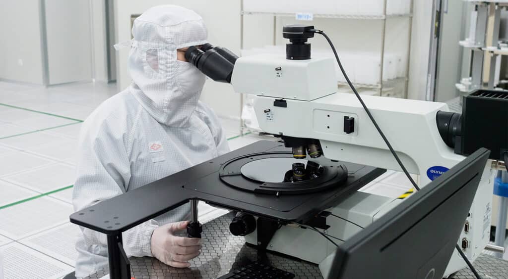
An optical microscope also known as a light microscope takes in visible light and uses lenses to show a magnified image through the eyepieces. This is what most people have in their heads when they think of a microscope. An optical digital microscope uses a digital camera for high-resolution imaging and then projects the image onto a monitor.
An optical digital microscope can give users a macro view, helping in the observation of large features and an overview of the entire wafer. While the magnification level is low, it is possible to observe contaminants through these images. The latest models have advanced features like automatic image processing for the combination of multiple high-resolution images to increase the field of view (FOV). With the use of zoom optics, users can easily magnify any feature of interest and go down to submicron resolutions.
Apart from the level of zoom available on a digital microscope, users can also select multiple observation settings at the touch of a button. The darkfield microscopy setting can reveal some defects with better clarity than using the brightfield image. There are also settings like differential interference contrast (DIC) and polarization to improve the contrast levels of the high-resolution images produced by a digital microscope.
Scanning Electron Microscope
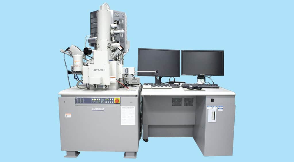
As integrated circuit components get smaller and increase in complexity, an optical digital microscope may not be sufficient to provide sufficient spatial resolution to detect contaminants. This is where scanning electron microscopy comes in. These microscopes use accelerated electrons to illuminate the material under observation instead of visible light. High-resolution images are then produced by detecting the reflected electrons or those that are knocked off.
Electrons are used because they have a shorter wavelength than visible light photos. This is what allows a Scanning Electron Microscope or SEM to obtain surface images at the atomic scale and reveal the structure of smaller components that an optical digital microscope cannot. Besides obtaining 3D images of surface structures that provide users with an idea of their geometrical arrangements, other SEM techniques reveal electrical or optical properties of the semiconductor materials.
Electron Beam Induced Conductivity
There is the Electron Beam Induced Conductivity (EBIC) method where an electron probe is used to generate charge carriers in the semiconductor material. Afterward, the recombination efficiency of the charge carriers is measured. This method can reveal inhomogeneities like crystal defects in semiconductor materials and is an essential part of semiconductor failure analysis.
Cathodoluminescence
In the Cathodoluminescence (CL) method, by analyzing emitted radiation resulting from the electron bombardment of the semiconductor material, users can identify radiative and non-radiative regions on the sample. Both panchromatic and monochromatic images can be taken, and by observing these, crystal defects can be found.
Scanning Deep Level Transient Spectroscopy
There is also the Scanning Deep Level Transient Spectroscopy (SDLTS) method. This technique involved analyzing the energy of electron states in the band gap of semiconductor materials. After the electron bombardment of the sample, capacitance transients are detected as a function of the temperature.
Often in the failure analysis of semiconductor materials, all three of these techniques are used in combination as they complement each other.
Transmission Electron Microscope
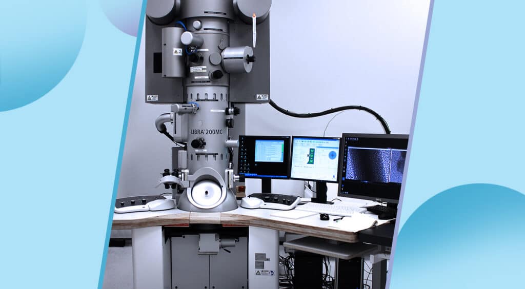
Transmission Electron Microscopes or TEMs are similar to Scanning Electron Microscopes (SEMs) since they both use electrons. Unlike SEMs which detect reflected electrons, TEMs transmit electrons through the specimen of semiconductor materials and then collected them onto an imaging device. What this does is enable users to obtain structural information from the inside of the material rather than from its surface.
The images produced by such a microscope are of a much higher resolution than those produced by optical microscopes. They can reveal a material’s interior crystalline structure, stress state information, and morphology.
Image Processing With Scanning Electron Microscope vs. Transmission Electron Microscope
The two types of electron microscopes are great at different failure analysis applications. Through image processing, SEMs allow users to get 3D images of the surface of the sample and are good at detecting contaminants. TEMs which show the interior structure are good at identifying impurities and structural defects. However, since the images produced by TEM image processing are in 2D, it is often a little challenging to interpret what they exactly show.
Since electrons have to be transmitted through the sample in TEM, the material under observation has to be less than 150 nanometers in thickness. For more high-resolution images that give even more detail, a sample must be no thicker than 30 nanometers, limiting what can be put under the microscope. The samples also need to be prepared through a complex procedure to ready them for imaging. Experienced handlers are needed to perform these procedures to ensure the sample does not produce any artifacts due to the preparation process.
There is no such thickness limitation for SEM and the sample of semiconductor materials can be readied for imaging with little to no preparation needed. They also require less voltage to accelerate electrons (about 30 kV) compared to the 60 to 300 kV needed for TEMs.
When it comes to the field of view or FOV, high-resolution images produced SEMs have a large FOV while TEMs only shows a small region of the sample. However, when it comes to magnification, SEMs can magnify only up to about two million times, whereas TEMs can provide a high-resolution image with 50 million times the magnification. SEM images achieve a spatial resolution of about 0.5 nanometers whereas TEMs can provide up to 50 picometers.
While SEMs are more cost-effective and require less training to use, one method of electron microscopy is not better than the other. They are used together in failure analysis of semiconductors and there are even some microscopes called STEMs that can combine the capabilities of both techniques.
Electron microscopy can potentially damage the wafer, and is usually used for research and development or failure analysis rather than for inspection during production. To learn more about why semiconductor devices fail, read Semiconductor Failure Analysis and Why It Is Important.
Short-Wave Infrared Microscope
Silicon which makes up the majority of semiconductor devices is transparent to infrared light. This means that a microscopic camera that operates in the 900 to 1700 nanometer range or short-wave infrared (SWIR) wavelengths can see through a silicon substrate. This inspection method is great because it is completely non-invasive. Indium Gallium Arsenide (InGaAs) cameras are used as inspection tools for failure analysis at various stages of the semiconductor manufacturing process.
Firstly, high-resolution SWIR cameras are used after the Silicon ingot growth phase to detect defects, impurities, and voids. It is very important to identify impurities at this stage since they can even damage the sophisticated equipment used in the next stage where ingots are cut into wafers. Later, after the silicon is processed into the wafer, the SWIR camera can be used again to detect particles and cracks that may be present inside the wafer or between two bonded wafers.
SWIR cameras can also be used for Photon Emission Microscopy, allowing users to observe sub-band gap emissions caused by chemical impurities and other defects like deep traps which regular CCD cameras cannot see. SWIR cameras are also used in the inspection of photovoltaic wafers used in solar panels.
Atomic Force Microscope
Atomic Force Microscopes (AFMs) can measure the surface structures of a Silicon wafer at the angstrom level which is 0.1 nanometers. The microscope uses a cantilever attached to a needle, and the tip of the needle scans the surface of the sample. While image processing is relatively slow compared to other types of microscopes, AFMs can produce 3D images with a resolution of 100 micrometers to 0.1 nanometers. It is also a non-invasive imaging technique that does not damage the sample its observing.
AFMs are usually used in combination with optical microscopes. If an unknown feature is discovered through the optical microscope, the AFM can then be pointed at this feature to identify what sort of defect it may be. Line profile analysis of a single scan line can reveal missing material on an integrated circuit. Through image processing, multiple line profiles can be combined to create a high-resolution 3D image which can provide an even better perspective into the defect. Color enhancement is also possible to make it easier to interpret the images.
Scanning Acoustic Microscope

The Scanning Acoustic Microscope (SAM) uses ultrasonic waves which can be used during one of the early steps in failure analysis where non-destructive methods are needed. Sound waves of the 5 to 150 MHz frequency range are transmitted through the semiconductor sample and their echos or the sound coming out the other side is detected and analyzed. Both 2D and 3D images with depth-specific information can be obtained, and defects such as voids, cracks, inclusions and delamination can be identified by studying these scans.
X-Ray Microscope
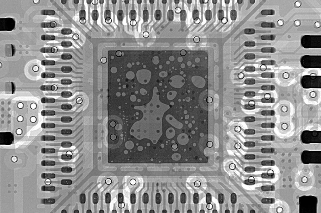
X-Ray microscopes are another non-destructive method for the analysis of semiconductor devices that fail. X-rays can give failure analysts a look at the internal structure of integrated circuit components and give an indication of their composition from the different ways the x-ray radiation passes through the sample. This can help them understand how to open the device for further examination.
Furthermore, x-ray images can be magnified by optical means, improving the spatial resolution and revealing defects like cracks in the die, contaminants and other anomalies. Through image processing of 2D x-ray scans from multiple angles, a 3D image can be constructed, giving further clues into the interior structure of a semiconductor device.
Who Makes Semiconductor Microscopes And Cameras?
There are many players in the semiconductor microscope and camera industry. Entities like Hitachi High-Tech Corporation, KLA Corporation, Thermo Fisher Scientific Inc, Onto Innovation Inc, and Applied Materials Inc are the companies that are at the forefront of research and development of inspection technology used by the semiconductor industry.
If your semiconductor manufacturing facility needs inspection tools for quality control and failure analysis, it is highly recommended you get the latest equipment from one of the above suppliers.
FAQs
A semiconductor microscope is a device used by manufacturers in the semiconductor industry for the inspection of Silicon wafers to detect impurities, defects, and contaminants at various stages of production.
Impurities, defects, and contaminants present in the Silicon wafers can render the integrated circuits manufactured from them unusable. They can also damage equipment used in the manufacturing process if not identified at the right stage.
There are many types of semiconductor microscopes each used for different applications in the inspection process. Optical microscopes, scanning electron microscopes (SEMs), transmission electron microscopes (TEMs), short-wave infrared microscopic cameras, and atomic force microscopes are the most commonly used for inspection.