Want to understand what dry etch semiconductor processing is all about? Find out all about the different types of dry etching techniques used in the semiconductor industry including plasma etching, reactive ion etching, and ion beam etching. Also find out what the difference is between wet etching and dry plasma etching, as well as the various factors to consider during the etch process.
What Is The Semiconductor Etching Process?
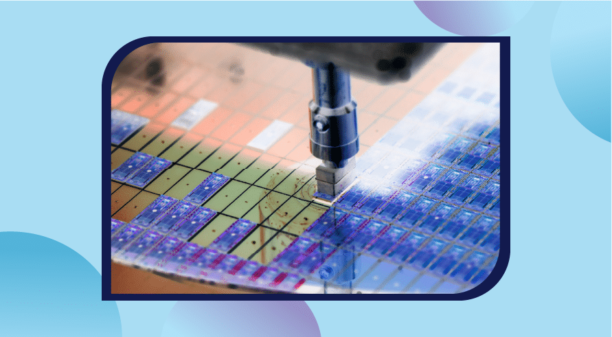
The etching process is an important part of semiconductor manufacturing where one or more layers of material are removed from a wafer surface. Based on the integrated circuit (microchip) layout required, sections of the wafer are protected by applying a masked pattern that is resistant to the etching agents. Sometimes this masking material is photoresist which is applied through the use of photolithography. More durable silicon nitride masks are also used.
There could be various steps in the silicon etching process based on the type of printed circuit boards (PCBs) or semiconducting materials that need to be produced. There are applications where the etching process is required to produce cavities on the wafer surface. The depth of this cavity can be controlled by adjusting the etch rate.
There are various etching processes, each with its own type of chemical etching agent. There is a form of dry etching called ‘plasma etching’. In this method, etch gases called ‘plasma’ are used to remove Silicon substrate material. Then there is wet etching where liquid chemicals are used instead. In addition to chemical etching through plasma, other dry etching processes utilize physical etching and a mix of the two.
Etching Characteristics To Consider During the Etching Process
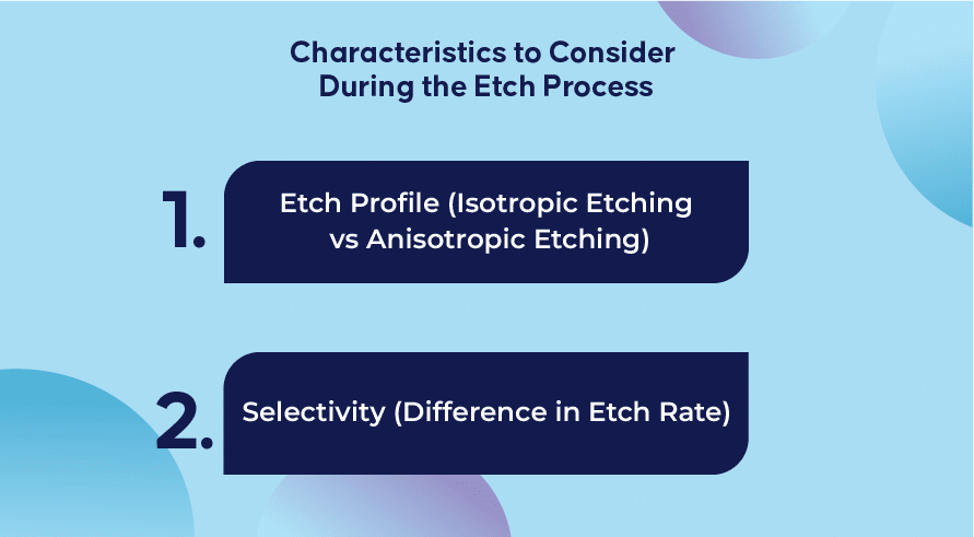
The etch process has to be very precise since it has to remove layers of semiconductor material from the exposed surface without damaging masked or underlying layers. As a result, there are two factors to be considered. The etch profile and etch rate.
In both wet and dry etching, manufacturers need to be aware of the direction of etching or ‘etch profile’. When the etching happens uniformly in all directions, it is called ‘isotropic etching’. However, if the etching removes material along a specific direction, this is called ‘anisotropic etching’.
The etching agents will etch different materials at different speeds. For example, the mask used for protection will have a different etch rate than the exposed material. The ratio between two etching rates is called ‘selectivity’, and this determines how chemical agents selectively etch one material but not the other. Liquids used in wet etching and plasma used in dry etching will have their own unique etch profile and etch rate making them suitable for different applications.
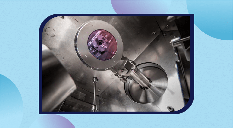
The Dry Etching Process
Dry etching is often used synonymously with plasma etching since it is one of the most widely used methods. However, there are other types of dry etching techniques used during semiconductor fabrication.
Plasma Etching Process
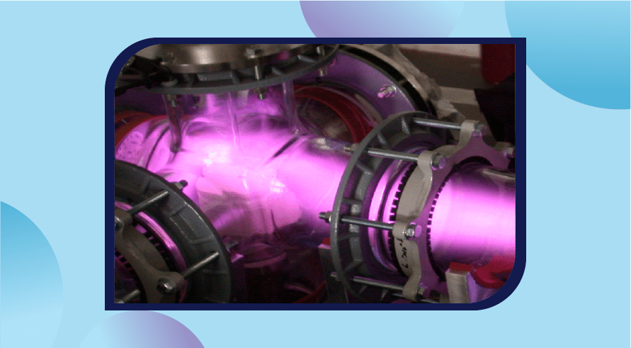
In plasma etching, reactive gases like oxygen, chlorine, or fluorocarbons are brought to a plasma state where they contain energetic and neutral particles called ‘free radicals’. These free radicals react with the surface of the substrate and etch out material. Since they react with the wafer from all angles, their etch profile is isotropic.
Different types of plasma etching are used depending on the substrate or material that requires etching. Carbon tetrachloride (CCl4) is used for silicon and aluminum. Hydrogen plasma etching is great for removing any native oxides found on the surface of the wafer.
A fluorine-based plasma can be used to remove a silicon dioxide film, while oxygen plasma etching is one of the most common ways to grow this. These methods are used in photolithography to selectively grow or remove photoresist material. Apart from semiconductor applications, oxygen plasma etching is also used in the deep-etching of diamond nanostructures.
Reactive Ion Etching (RIE) Process
Reactive ion etching is a form of plasma etching. However, using a radio frequency (RF) signal, free electrons, and positively charged ions are now created within the plasma in addition to the free radicals. The charged ions can be accelerated by applying a separate RF signal. These accelerated ions strike the wafer surface at a perpendicular angle, and if they have sufficient energy, are capable of knocking material out of the substrate even without a chemical reaction.
Accelerated ions are used to physically etch the surface, and this process is directional, making it anisotropic. The depth of the etching and the etch rate can be controlled by adjusting the frequency of the RF signal. The free radicals react with the wafer surface as usual with isotropic etching. They also ensure that any material etched out by the ions cannot be redeposited on the wafer.
Since the RIE method of plasma etching has both physical and chemical etching aspects, its directional aspects can be controlled by adjusting various parameters like the pressure in the etching chamber, temperature, and frequency of the radio wave. A more advanced form of RIE plasma etching is Deep Reactive Ion Etching (DRIE) which promises deeper etching than ever before with nearly vertical sidewalls. This is done through the ‘Bosch Process’ where different compositions of etching gases are used in an alternating fashion.
Ion Beam Etching Process
Ion beam etching is purely a physical form of dry etching. The wafer is bombarded with positive ions of a noble gas which is usually Argon. Here, the kinetic energy of these accelerated argon ions causes the dry etching of the surface. Since the positive ions are directed perpendicularly to the wafer, the process is anisotropic, although the downside is that there is very low selectivity since the ions cannot differentiate between different layers.
Another issue is that etched material may deposit on the wafer since they are not in a gaseous state. This combined with the low selectivity and low etch rate makes ion beam dry etching a process that is rarely used anymore. Plasma etching with RIE or DRIE methods is far superior and is much more flexible.
What Is Wet Etching?
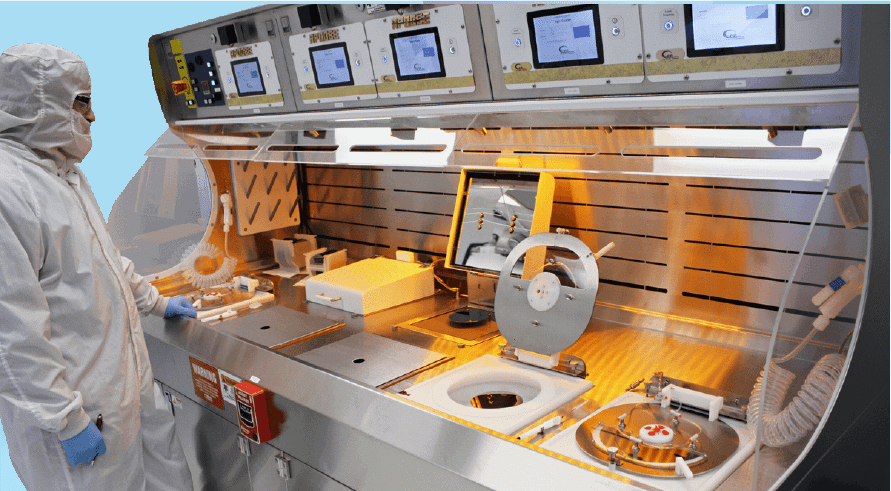
Wet etching is a form of chemical etching, but unlike plasma etching, uses liquid reactants. These chemicals can be acidic or basic depending on the substrate to be etched. The substrate is sprayed or immersed in a tank that contains the chemical. It then selectively etches the exposed parts of the substrate. Wet etching has very high selectivity, with the ability to use thin masks and even halt quickly after one layer is etched without damaging the next one.
Masks are used frequently in wet etching and need to be carefully selected. They have to be resilient to not being dissolved or etch slower than the exposed parts of the substrate. Hydrofluoric acid is used for silicon substrates and hydrochloric acid for gallium arsenide.
Wet etching is isotropic and tends to undercut the mask. This creates features that are larger than the mask. Furthermore, wet etching also results in very large amounts of industrial toxic waste which requires safe disposal. To learn more about the equipment used in wet etching, read Semiconductor Wet Processing Equipment
Wet Etching vs Dry Etching
Apart from the state of the substances used in the etch process, dry etching and wet etching differ in many significant ways.
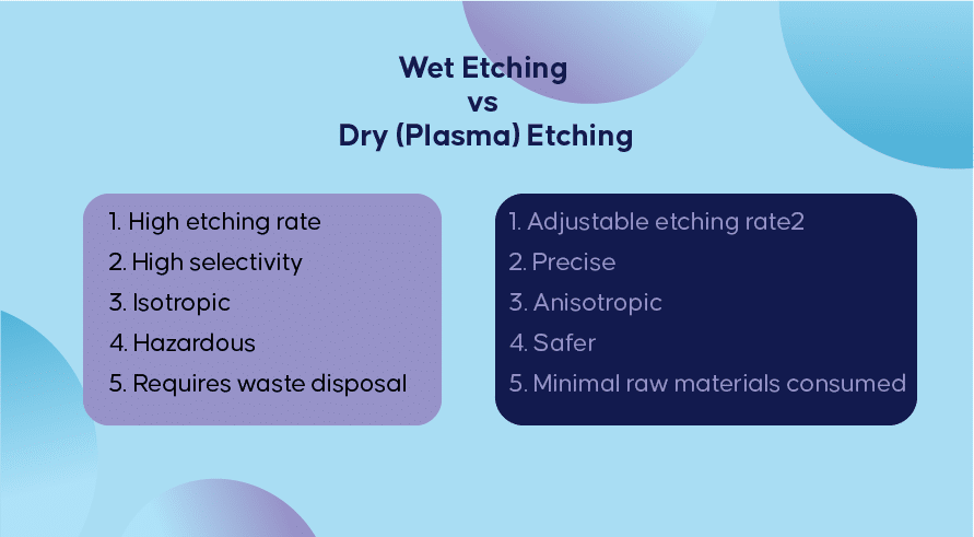
Wet etching is relatively quick with a high etching rate. A high level of selectivity can be obtained with very simple equipment such as chemical baths and spray systems. Selectivity is good to ensure it only removes the unwanted material from the substrate while leaving the rest unharmed. However, wet etching can be hazardous since we are dealing with corrosive and highly toxic chemicals. Not only do they need to be replenished continuously to maintain the etching rate, but they also need special disposal systems which can be costly. Furthermore, special filtering systems are needed to be installed on the workbenches to remove toxic fumes to maintain a safe environment for the engineers.
Dry etching in comparison is much safer and the plasma treatment is carried out in a special vacuum chamber called an ‘etching chamber’ far away from the plant engineer. Dry etching can be very precise as well with the ability to control the depth and rate of the etching by adjusting the frequencies of the radio wave. Different types of plasma treatment from oxygen plasma to hydrogen-based ones can be used with a wide range of process settings available using the same equipment. Minimal raw materials are consumed in dry etching, and a majority of the gaseous waste products are non-toxic.
Etching Applications
No matter which methods are used, etching semiconductors is an important step in the manufacture of integrated circuits and printed circuit boards. Apart from manufacturing applications, etching is also used in the analysis of failed devices.
Plasma Etching For Semiconducting Materials
Plasma etching is utilized extensively to prepare semiconducting materials to be used for the production of integrated circuits. Microscopic features can be etched onto the surface of a substrate to alter its electrical properties. Microelectromechanical systems or MEMS are microscopic devices with moving parts that require plasma treatment to produce deep trenches on Silicon surfaces to make them work. Scientists at the forefront of this technology are now attempting to utilize plasma etching for even tinier MEMS devices at the nanometer scale.
Etching For Printed Circuit Boards

Etching is also used to remove the excess copper when manufacturing printed circuit boards (PCBs). Before the etching begins, the layout of the desired circuit is created. This circuit layout is transferred to the board using photolithography. There are two etch resists in this procedure, the outer tin plating which marks the border, and the photoresist which marks the circuit blueprint. The exposed base copper, also known as the ‘start copper’ is then removed through the etching process. Both dry and wet etching methods may be used for this purpose.
Delayering In Semiconductor Failure Analysis
An integrated circuit may sometimes fail during operation. When this happens, they are analyzed by scientists to determine the cause of failure which could be manufacturing defects, anomalies, contamination, or other reasons. To do this, the integrated circuits need to be opened to check their internal structures. The process of removing outer layers is called ‘delayering’. Both dry plasma etching and wet chemical etching are used depending on the material that needs to be removed. For more on this topic, read Semiconductor Failure Analysis and Why It Is Important.
New Dry Etching Techniques For Next-Generation Semiconductor Devices
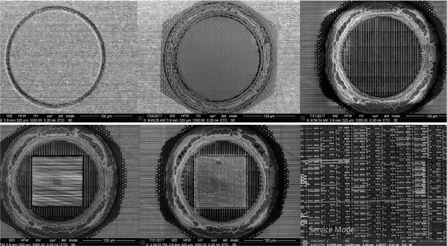
A study published in the ACS Omega journal showed the potential of new plasma etching techniques that will become invaluable for the development of next-generation semiconductor devices. Sulfur hexafluoride and oxygen plasmas have been tested in a plasma etching process with a novel approach called ‘interferometric endpoint detection’ (IEPD).
In this technique, the trench depth on the surface of silicon carbide could be accurately controlled. The quality and uniformity of the trenches were later verified using transmission electron microscopy (TEM) and X-ray photoemission spectrometer methods. For more on the advanced equipment used to study semiconductor components, read What Does A Semiconductor Microscope Do?
This research showed minimal surface modification of silicon carbide with no fluoride poisoning, indicating the potential for producing future devices using dry plasma etching techniques. To learn more about semiconductor devices, how they are manufactured, and their applications, check out Inquivix Technologies!
FAQs
Dry etching is a semiconductor manufacturing process where the material is removed from a semiconductor substrate using plasma instead of liquid chemicals.
Dry etching using plasma is anisotropic, providing greater control of the etching rate and depth. It is also safer to handle, consumes fewer raw materials, and creates less toxic waste compared to wet etching with chemicals.
Yes. Wet etching is a quicker process due to its faster etch rates and is highly selective compared to dry etching.