
If you wish to learn how the electrical properties of semiconductors arise, then you need to first understand the chemistry of semiconductors. Find out what makes a semiconductor different from a conductor or insulator, and how band theory can be used to explain the electrical characteristics of different semiconducting materials. You’ll also understand the role charge carriers like electrons and holes have, and what happens in the P-N junction of a diode. Let’s begin!
Table of Contents
What Are Semiconductor Materials?
One of the most significant achievements in physics and solid-state inorganic chemistry is the development of semiconductors. Since the invention of the transistor in 1947, various types of semiconductor devices have appeared over the decades with a wide array of applications. Any modern piece of technology from the smartphone in your pocket to the most advanced scientific instruments used by astronomers like the James Webb space telescope utilizes integrated circuits to function.
The electrical properties of these integrated circuits or microchips arise from the semiconducting materials that are used to manufacture them. A modern microprocessor like the ones found in Apple’s iPhones has billions of tiny transistors packed into it.
A semiconducting material has an electrical conductivity that is between a conductor such as copper, and an insulator like glass. Unlike a metal which increases in electrical resistivity with temperature, semiconductors do the opposite. Semiconducting materials include pure elements like Silicon and Germanium, as well as compounds like Gallium Arsenide.
Semiconductor Theory: Band Theory
At present, the electrical conductivity of semiconductors is explained by the band theory. According to band theory, the electrons in a solid material are distributed into energy bands among all the atoms that make up the material. Each energy band has a different energy level and the electrons occupy these energy levels from lowest to highest. These energy band structures are unique to each type of material. This is the reason why the electrical conductivity of a semiconductor is different from that of a conductor or electrical insulator.
Valence Band
The valence band is the highest energy band that contains electrons. In a conductor like copper, the valance band is partially filled with electrons. These valence electrons are free to access unoccupied spaces within the valence band, giving them mobility across the solid material. When a voltage is applied, these electrons begin to flow, and an electric current is generated.
In electrical insulators, the valence band is completely filled with electrons, allowing no mobility for electrons to move and generate a current. Silicon which is the most widely used semiconductor material has four valence electrons.
Conduction Band
The conduction band is the lowest energy band that is empty and contains no electrons. According to the energy band structure, the conduction band is situated above the valence band, and the energy gap between them is called the band gap. According to quantum mechanics, electrons cannot stay within band gaps, and therefore have to be located in the conduction band or valence band.
Jumping The Band Gap With Thermal Energy
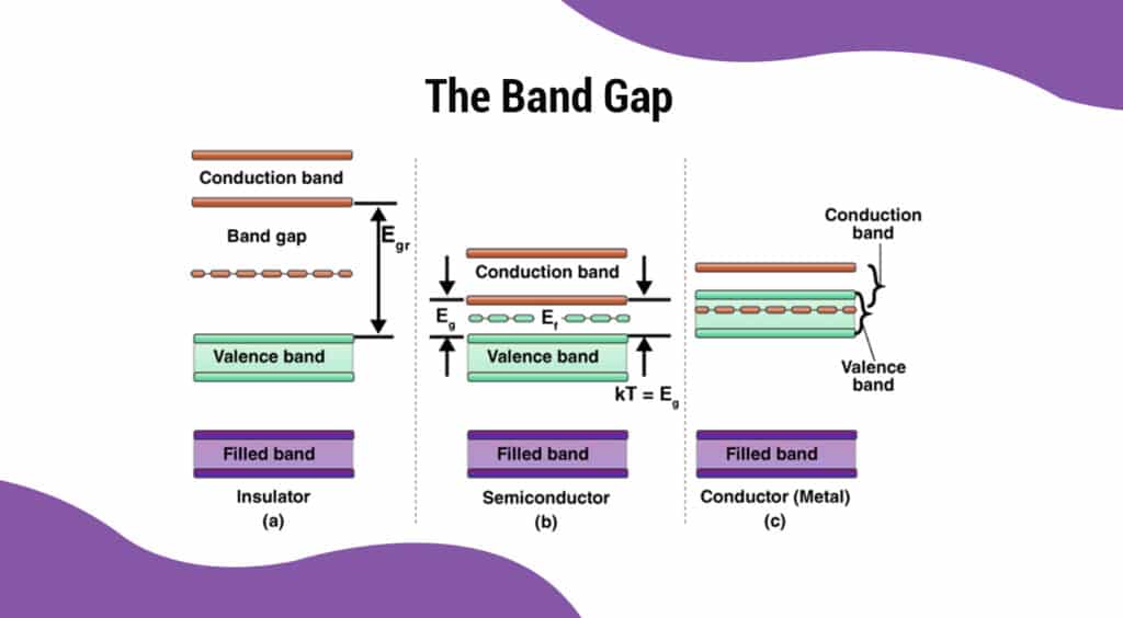
Electrons from the valence band can be excited to jump into the conduction band by providing the solid material with thermal energy (heat). This would result in a conduction band that is partially filled with electrons and holes which are positive charge carriers resulting from vacated electrons in the valence band. A partially filled band can facilitate the conduction of a current.
In electrical insulators, the valence and conduction bands are too far apart. In other words, it would require far too much energy to excite any electrons to jump the energy band gap. This is not practical. The band structures of semiconductors are such that the band gap between the conduction band and the valence band is not too far apart. Even a small amount of heat at room temperature could excite the valence electrons to jump into the conduction band. The electrical conductivity of semiconductors increases with heat as more and more valence electrons jump into the conduction band.
Types Of Semiconductor Materials
Semiconductors exhibit the electrical properties of both conductors and insulators. These properties can be adjusted at need by changing the chemical composition of semiconductors materials which can be broadly classified into the two following categories.
Intrinsic Semiconductors
An intrinsic semiconductor is a pure semiconductor, made from only one type of semiconducting material. Silicon (Si) and Germanium (Ge) are the most widely used of this type. They are also called ‘undoped semiconductors’ or ‘I-type semiconductors’.
Extrinsic Semiconductors
Other types of elements can be introduced to an intrinsic semiconductor through a process called ‘doping’. It would no longer be a pure semiconductor anymore and its chemical properties will also change as a result. These are referred to as ‘extrinsic semiconductors’ and have slightly different electronic properties. An extrinsic semiconductor can be of two types, depending on the kind of charge carriers that are created within it.
N-Type Semiconductors
In an N-type semiconductor, the atoms introduced from the doping process add extra electrons into the conduction band. These ‘electron donor’ elements can be found on the right side of Silicon in the periodic table. Phosphorus is a common choice of material to dope Silicon since it contains one extra electron it can donate to Silicon. Since electrons are negative charge carriers, this type of semiconductor is known as an N-type semiconductor.
P-Type Semiconductors
In a P-type semiconductor, the charge carriers will be holes. This is done by adding an element with missing valence electrons. The absence of electrons makes these holes positive charge carriers, hence the name ‘P-type semiconductors’. This type of element is an ‘electron acceptor’ and is found to the left of Silicon on the periodic table. Boron is a common element used with Silicon to make a P-type semiconductor.
How Electrical Properties Of Semiconducting Material Are Used To Build Electronic Devices

An N-type semiconductor and a P-type semiconductor are both used to make one of the most basic electrical junctions known as a ‘P-N Junction’. These P-N junctions are formed from the interface between P-type doped regions and N-type doped regions. Through diffusion, electrons and holes from the two sides combine to form a region where there are no charge carriers. This is the ‘depletion region’ at the center of a P-N junction.
On one side of the depletion region are electrons from the N-type material and on the other are holes from the P-type semiconductor. This charge separation creates an electrical barrier that prevents any further movement of electrons across the junction. A P-N junction will only allow electrons from the N-type region to move to the P-type side if they can overcome the energy barrier of the depletion region. These semiconductor devices are called ‘diodes’.
When a forward bias (positive voltage) is applied to the P-N junction, the energy barrier is lowered, allowing conduction band electrons on the N-type side to flow across the junction. As a result, an electric current is generated. When a reverse bias is provided to the junction, the depletion region grows and the charge separation is greater. As a result, the energy barrier is increased, further preventing electrons from crossing over. No current can flow from the P-doped region to the N-doped region in a diode.
Since diodes restrict electrical conductivity to one direction, their logic was used to replace vacuum tube technology. Logic gates like AND as well as OR gates are examples of this. Later, more complex transistors were developed such as NPN and PNP which were more sophisticated than a standard diode. Their properties made the binary logic of zeroes and ones used by modern computers possible.
Optoelectronic Devices
Semiconductor devices have other physical properties beyond just allowing or restricting a current to flow through them. Some types of semiconducting material can take electrical energy and convert it into light energy. Others can absorb light and turn it into electrical energy. These are referred to as ‘optoelectronic devices’.
Light Emitting Diodes
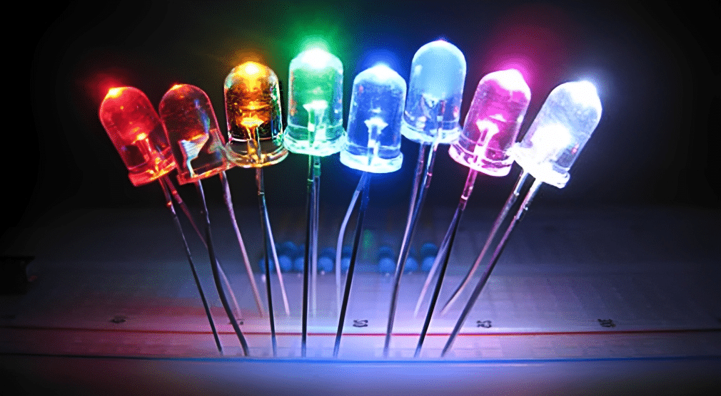
Light-emitting diodes or LEDs are perhaps the most common type of optoelectronic device that has been around for decades. They are used in all types of electronic devices to display information or to provide lighting. When a forward bias is applied to the junction in an LED, electrons in the conduction band and holes in the valence band move and begin to combine. The result is the energy released as visible light.
The wavelength of light released depends on the band gap of the semiconducting material used. Silicon doesn’t exhibit this quality, creating heat instead of light. Materials such as Gallium Arsenide (GaAs) exhibit light-emitting characteristics and are called ‘direct gap semiconductors’.
Photodetectors And Solar Cells

Photodetectors and solar cells work in the opposite way to LEDs. They are called photovoltaic systems. The light energy that falls on the P-N junction is absorbed by valence electrons which jump up to the conduction band. Electrons travel to the N side and holes travel to the P side of the junction. Current flows as a result of moving charge carriers. Light energy is converted to electrical energy.
Some photovoltaics are great at detecting light, and these are used cameras and imaging systems. Others are good at storing the energy converted. These are the solar cells found in solar panels.
Fabrication Of Semiconductor Devices

The semiconductor industry employs some of the most advanced manufacturing technologies available today to fabricate semiconductor materials. A dopant such as Phosphorus is added to high-purity molten Silicon. N-type Silicon crystal is grown as ingots and sliced into thin disk-shaped pieces called ‘wafers’.
Photolithography techniques are used to create a layer of Silicon Dioxide on the surface of the wafer and parts of this layer are etched away to expose specific areas. These exposed regions are then bombarded by Boron ions which build up the P-type regions on the wafer. Through a combination of deposition, etching, and ion implantation, the required electronic structure of the integrated circuit can be created on the wafer surface.
Today, hundreds of microchips can be created on a single semiconductor wafer with the most advanced processors found in smartphones now capable of holding billions of transistors within a tiny area just a centimeter across. Finding ways to fit even more components into increasingly tiny surface areas is an ever-present challenge in the semiconductor manufacturing industry.
How Chemistry Is Impacting Semiconductor Material At the Nanometer Scale
The increasing miniaturization of integrated circuits puts even more pressure on the chemistry that enables semiconductors to behave the way they do. We are now approaching the atomic level scale where exact quantities of atoms can have an impact on how a logic gate will function. Films used as insulating materials are now less than 50 atoms thick, and increasingly better precision is needed to handle these.
The photoresist materials also need to have precise distributions of particles within them, and when their role is done, need to be removed. This removal needs to be done carefully so that no contaminants are left over to cause issues later. The substrate didn’t traditionally factor in much when it came to electrical signals. However, this has changed and its chemistry can cause noticeable issues with these signals if it contains any imperfections.
Sophisticated imaging techniques are used to ensure that no contaminants or manufacturing defects can compromise the integrity of the wafers.
FAQs
The band gap is the energy gap between the valence band and the conduction band of a solid material.
For charge carriers to move and generate a current when a voltage is applied, the valence band has to be partially filled with electrons like in a conductor or the electrons need to be excited to the conduction band like in a semiconductor.
The Silicon atom has four valence electrons allowing it to make covalent or ionic bonds. This flexibility makes it easy to adjust its semiconducting electrical properties by combining it with other elements. It is also found in abundance on Earth and is a relatively inert element that does not react with water or oxygen as a solid.