
Semiconductor devices are used in a huge range of consumer electronics and other products. In order to keep up with demand, semiconductor fabrication plants (factories) require a large number of these devices. To increase throughput and efficiency, factories use FOUP handlers to move wafers safely from one manufacturing step to the next. If you’re curious about what FOUPs are and how they work, read on! We’ll answer all your questions and more.
What Is FOUP?
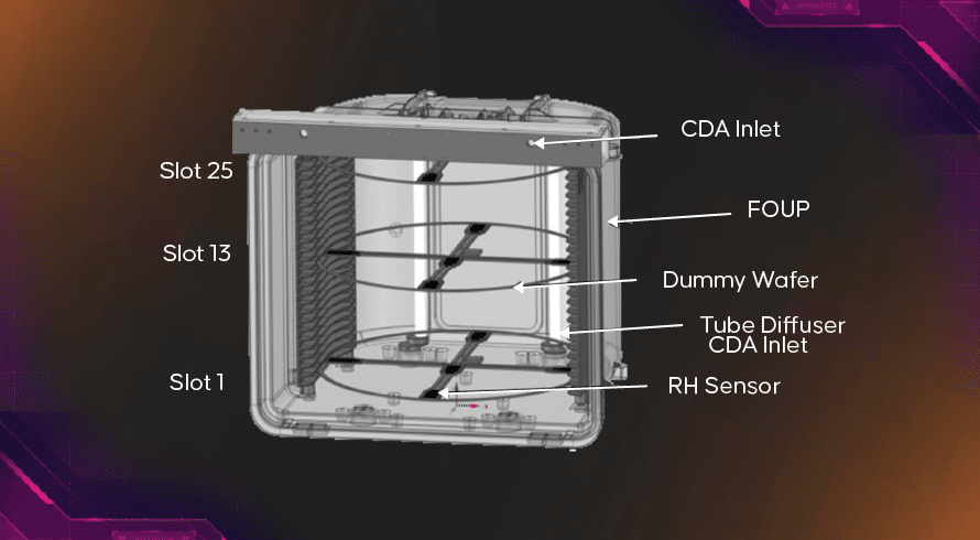
FOUP which is the acronym for Front Opening Unified Pod or Front Opening Universal Pod is a special tool used to handle semiconductor silicon wafers. These are plastic chamber-like boxes or enclosures that are used as a transport medium to move around semiconductor wafers during the manufacturing process.
These wafer carriers have been around since the latter half of the 1990s and have undergone various changes according to the different requirements that time, technology, and demand have brought about. There are many factors to consider when building this device to ensure that the wafer is under a high level of cleanliness and to minimize any external particles that may damage the wafer as it is transported. Below we have explained the factors taken into consideration to make the FOUP effective.
Factors Considered When Building Front-Opening Unified Pods
In the 1990s, these front-opening unified pods were built simultaneously with the introduction of 300mm wafer processing equipment. Using these wafers directly in semiconductor wafer fabrication and cleanroom environments was difficult due to their size and susceptibility to being easily damaged or polluted. Here are the factors that were considered when front-opening unified pods were developed.
The 300mm Constraint
So, front-opening unified pods were built taking into consideration the 300mm size constraint. Fins were used to secure the wafers instead of portable cassettes.
Robot-Friendliness
The opening doors were initially not even front-opening. The door was changed to open from the front instead of the bottom to enable direct handling of the wafer for robots.
Must Allow AMHS (Automated Material Handling System)
Most completely filled FOUPs are extremely heavy, with a 25-wafer FOUP recording a staggering measurement of up to nine kilograms. With respect to this, the wafer storage must allow for automated material handling systems to transport it.
A 10mm pitch is required for a 300mm front-opening unified pod. On the other hand, a 19mm pitch can accommodate 13 wafers. To smoothly haul the FOUP, it will need a diverse combination of coupling plates, pins, and holes. Radio-frequency tags may also be required to be easily classified in the AMHS processing.
Adaptable To Higher Yield Production
If devices are expected to produce a higher yield, FOUPs can have a nitrogen environment surrounding them.
These are just some of the many factors considered when manufacturing FOUPs. Why is the manufacturing process of a FOUP so important for semiconductor wafers? We’ve explained it all in detail below.
The Importance Of Front-Opening Unified Pods
The semiconductor wafer is one of the most important components of the semiconductor fabrication process. The front-opening unified pods are important because it is the wafer carrier. However, there are many reasons for its importance and we have outlined some of them below.
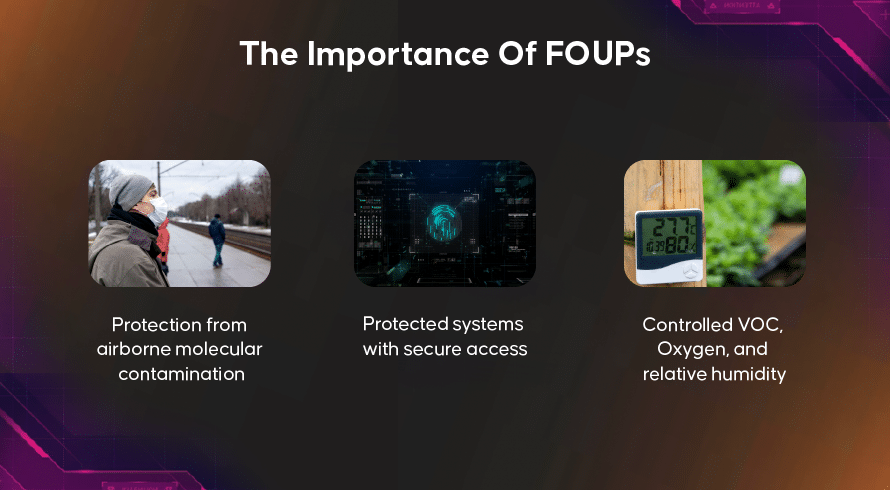
Protection From Airborne Molecular Contamination
The main reason is that wafers are susceptible to chemical reactions which may cause them to be exposed to any form of contamination. This will result in short circuits or circuit damage. A FOUP protects the wafer from undesired reactions as the wafer awaits the next step in its fabrication process.
Protected Systems With Secure Access
FOUPs ensure that the wafer manufacturing is automated so that there is little manual labor involved. This ensures there is little room for error within the automated system followed and allows for a secure and accurate wafer fabrication process. A purging process is also carried out with an inert gas to protect the wafer from molecular contamination through air and the water surface.
Controlled VOC, Oxygen, And Relative Humidity
Exposure to volatile organic compounds (VOC), oxygen, and humid conditions are factors that greatly affect the wafer’s fabrication. With FOUPs, only the required compounds and elements are allowed within a closed and controlled system. This is essential for the success of the semiconductor devices developed from these wafers and their future applications.
Get Your Semiconductor Components From A Trusted Partner
FOUPs are essential to the wafer and semiconductor fabrication procedure. It ensures that the final products are of high quality and can be used for years after production with circuit damage. It is the most secure device to store wafers as they move from machines to different steps. These factors make it very vital that manufacturers maintain high standards when building a FOUP.
At Inquivix Technologies, we provide high-quality semiconductor components from South Korea. If you are looking for a reliable partner to get you the necessary components, contact us and get a quote.
FAQs
FOSP is a front-opening shipping box used to transfer the wafer from the wafer fabrication unit to the semiconductor manufacturing unit. On the other hand, FOUP is a front-opening unified pod that stores and moves the wafer from one process to another in the semiconductor factory.
It is a device installed at the entryway of the semiconductor fabrication system which collects the FOUP from the operators or AMHS/PGV systems that transport it. It is used to clamp, dock, and undock the FOUP and then open and close the door leading to the wafer.